
Master USB-C PCB layout with 12 essential design rules covering differential pair routing, impedance control, power delivery, and ESD protection. Practical engineering guide for reliable high-speed designs.
One incorrect USB-C PCB layout can cause intermittent charging, unstable USB enumeration, failed DisplayPort output, or complete USB4 link failure. Most of these issues are not caused by the connector itself—they originate from PCB routing, impedance control, grounding, or footprint design.
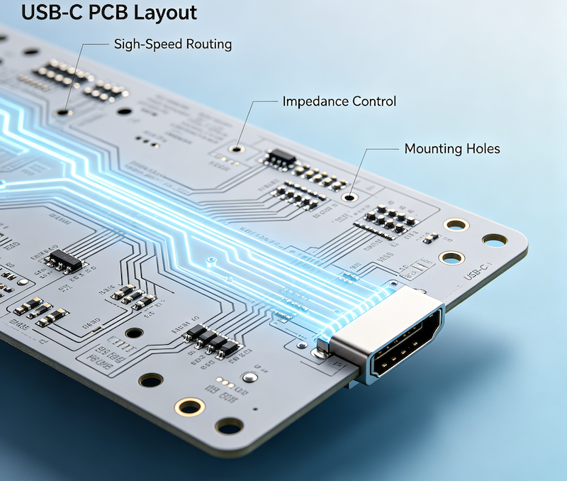
This guide walks through the essential design rules for reliable USB-C PCB layouts, from footprint creation through high-speed differential pair routing and power delivery implementation.
1. Before PCB Layout: Choose the Right USB-C Connector
The connector you select determines the entire layout strategy. USB-C connectors come in multiple pin configurations and mounting styles, each with different routing implications.
| Pin Count | Typical Use Case | Routing Complexity |
|---|---|---|
| 6-pin | Charging only, USB 2.0 data | Low |
| 9-pin | USB 2.0 + PD | Low to Medium |
| 16-pin | USB 3.1 / 3.2 (one SuperSpeed lane) | Medium |
| 24-pin | USB4 / Thunderbolt (dual-lane) | High |
Mounting style also matters. Mid-mount connectors sit lower on the board, vertical connectors route straight down, and right-angle connectors require careful fanout planning.
Selecting the wrong connector before layout starts often forces compromises that degrade signal integrity. The USB-C connector category page covers the full range of options available. For detailed selection criteria, the USB-C Selection Guide walks through technical specifications and application scenarios.
2. USB-C Footprint Design
Footprint errors are among the most common—and most expensive—mistakes in USB-C PCB layout. A connector that doesn’t sit flat, pads that are too small for reliable soldering, or mechanical interference with the board edge can scrap an entire production run.
Critical Footprint Elements
Pad Dimensions – USB-C pins are tightly spaced at 0.5mm pitch. Pad dimensions must match the connector datasheet exactly. Even a 0.1mm deviation can cause tombstoning or poor solder joint formation.
Shell Pads – The connector shell requires large, thermally-relieved pads for mechanical strength and proper grounding. Insufficient shell pad size leads to weak mechanical retention and poor EMI performance.
Anchor Pads – These provide mechanical stability during insertion and removal cycles. Anchor pad placement must match the connector’s mechanical drawing precisely.
Keepout Areas – Most USB-C connectors require keepout zones on inner layers beneath the connector body to prevent short circuits and ensure proper seating.
Courtyard – The component courtyard defines the minimum clearance around the connector for assembly. This must accommodate pick-and-place nozzle clearance and reflow soldering requirements.
Paste Mask – Stencil aperture design affects solder paste volume. For 0.5mm pitch pins, typically a 1:1 aperture with slight reduction for fine-pitch applications works well.
Footprint Verification Protocol
Before committing to production:
- Print the footprint at 1:1 scale and physically place the connector on the paper
- Run DRC with the connector’s mechanical drawing overlaid
- Confirm via clearance—vias should not fall under the connector body unless specified
3. PCB Stack-up Recommendations
The stack-up determines what impedance values are achievable and how much routing flexibility you have. For USB 2.0 only, a 4-layer board can work. For USB 3.x and above, 6 layers is the practical minimum.
Minimum Layer Count by USB Generation
| USB Generation | Minimum Layers | Recommended |
|---|---|---|
| USB 2.0 (480 Mbps) | 2 | 4 |
| USB 3.2 Gen 1 (5 Gbps) | 4 | 6 |
| USB 3.2 Gen 2 (10 Gbps) | 6 | 8 |
| USB4 (40 Gbps) | 6 | 8+ |
Recommended 6-Layer Stack-up
Top Layer      – Signal (high-speed differential pairs)
Layer 2        – GND (continuous reference plane)
Layer 3        – Power / Signal
Layer 4        – GND (continuous reference plane)
Layer 5        – Signal / Power
Bottom Layer   – Signal (low-speed / CC / SBU)
High-speed differential pairs should reference continuous GND planes. Splitting or cutting the ground plane increases electrical noise and jitter on USB signals.
For USB4 designs, material selection matters. Standard FR-4 may not meet insertion loss budgets at 40 Gbps. Low-loss materials like Megtron 6 or Panasonic M6 are often required. Work with your PCB fabricator on stack-up calculations before routing begins.
4. Differential Pair Routing
This is where most USB-C PCB layout issues originate. USB4 requires 85Ω ±5% differential impedance—not the traditional 90Ω used for USB 3.x. USB4 specifications recommend 80-85Ω controlled impedance for high-speed differential pairs.
Critical Differential Pair Rules
Impedance Control – 85Ω differential for USB4, 90Ω for USB 3.x. Define net-specific impedance rules in your CAD tool before routing begins.
Length Matching (Intra-Pair) – P and N signals within a pair must match within ≤0.15mm. This ensures differential signals arrive simultaneously to cancel common-mode noise.
Length Matching (Inter-Pair) – TX pairs must match each other, and RX pairs must match each other, typically within ≤1.0mm.
Pair Spacing – Follow the 3W rule: edge-to-edge spacing between adjacent differential pairs ≥3× the differential trace width.
Reference Plane – Route differential pairs over continuous GND planes. Avoid routing over splits or voids. USB4 traces should not be routed over voids or reference plane splits.
Via Usage – Minimize vias on high-speed differential pairs. Each via adds impedance discontinuity and parasitic capacitance. If vias are unavoidable, limit to ≤2 transitions per pair.
Back-Drilling – At 40 Gbps, even a stub longer than 10 mil can cause significant reflections. Back-drilling or HDI laser vias are required for USB4 layouts.
Routing Sequence Priority
- USB4 / SuperSpeed differential pairs (highest priority)
- USB 2.0 differential pair (D+/D-)
- CC1/CC2 (configuration channels)
- SBU1/SBU2 (sideband use)
- VBUS power
5. USB-C Connector Fanout
Fanout strategy determines how signals escape from the connector’s tight 0.5mm pitch. Poor fanout creates routing nightmares later.
Fanout Methods
Dog-Bone Fanout – Traditional method using short traces from pads to vias. Works for larger pitch connectors but consumes board space.
Direct Routing – Route traces directly from pads without vias for signals on the same layer. Preferred for top-layer routing.
Micro-Via Fanout – Use laser-drilled micro-vias directly in pads for HDI designs. Allows routing on inner layers immediately.
Escape Routing – Route signals out from the connector in a structured pattern. High-speed pairs should escape symmetrically to maintain length matching.
Fanout Best Practices
- Route high-speed differential pairs out first
- Keep differential pairs together through the fanout region
- Avoid necking down trace widths in the fanout area
- Place GND vias adjacent to signal vias for return current paths
6. Grounding
Grounding is the foundation of signal integrity, yet it’s frequently treated as an afterthought. Proper grounding requires attention to three areas: shell connection, return current paths, and stitching vias.
Shell Grounding
The connector shell should be connected to the PCB ground plane through multiple vias placed close to the shell pads. This provides:
- Low-impedance return path for common-mode currents
- Shielding against EMI
- Mechanical strength
Some designs use a resistor or capacitor between shell and ground to control ground loops. For most applications, direct connection through multiple vias is preferred.
Return Current Path
High-speed signals must have a clear return current path directly beneath the trace. Return currents follow the path of least inductance—which is directly under the signal trace on the reference plane.
Never route high-speed signals over split planes. The return current must detour around the split, increasing loop area and radiation.
Stitching Vias
Place GND vias around high-speed differential pairs to create a Faraday cage effect. Stitching vias should be spaced no more than λ/10 apart (approximately 1-2mm for USB4 frequencies).
All ground return pins on the USB-C connector should be bussed together on the PCB.
7. Power Delivery Layout
USB Power Delivery (USB PD) introduces high-current challenges that many engineers underestimate. At 5A and 20V (100W) or 5A and 48V (240W for PD 3.1), VBUS routing becomes a critical thermal and electrical design consideration.
VBUS Routing Guidelines
Trace Width – Calculate trace width based on current and allowable temperature rise. For 5A, use minimum 2mm (80 mil) traces or copper pours.
Via Count – Use multiple vias in parallel for VBUS connections. A single via typically handles 1-2A; for 5A, use at least 3-4 vias.
Voltage Drop – The most common cause of voltage drop failure in USB PD is resistance associated with the VBUS trace. Budget for voltage drop based on trace length and current.
Decoupling Capacitors – Place bulk capacitors for VBUS power close to the connector. These provide local charge storage during current transients.
Thermal Management – High-current paths generate heat. Use copper pours rather than traces, and consider thermal vias to inner layers for heat spreading.
CC Line Routing
The CC (Configuration Channel) pins are critical for PD negotiation. CC lines should be:
- Routed as 5.1kΩ pull-down to GND
- Kept short and away from noise sources
- Protected with ESD diodes
8. ESD Protection Placement
ESD protection devices must be placed as close to the USB-C connector as possible—ideally within 1.5mm. The standard placement sequence is: ESD → common-mode choke → resistors/capacitors.
ESD Device Selection Criteria
| Parameter | Requirement |
|---|---|
| Clamping voltage | ≤6V |
| Capacitance | Low (<1pF for SuperSpeed lines) |
| Compliance | IEC 61000-4-2 |
| Number of channels | Match signal lines protected |
Place ESD diodes on:
- All SuperSpeed differential pairs (TX/RX)
- USB 2.0 D+/D- lines
- CC1/CC2 lines
- SBU1/SBU2 (if used)
9. USB4 PCB Layout
USB4 at 40 Gbps is fundamentally different from lower-speed USB designs. The design rules above become mandatory requirements, not recommendations.
USB4-Specific Requirements
| Parameter | USB4 Requirement |
|---|---|
| Differential impedance | 85Ω ±5% |
| Intra-pair skew | ≤0.15mm |
| Inter-pair skew | ≤1.0mm |
| Via transitions | Minimize; back-drill required |
| Channel loss | Strict budget; low-loss materials required |
| Reference plane | Continuous; no voids |
USB4 uses dual-lane operation, meaning two full SuperSpeed pairs in each direction (TX1/TX2 and RX1/RX2). All four pairs must meet the same stringent requirements.
USB4 Material Selection
Standard FR-4 is marginal at 40 Gbps. Consider:
- Megtron 6 – Common choice for USB4 designs
- Rogers RO4350B – High-performance alternative
- Panasonic M6 – Low-loss material
Work with your PCB fabricator to confirm material availability and pricing before committing to a design.
10. Common PCB Layout Mistakes
These mistakes appear repeatedly in design reviews. Avoiding them saves time, money, and frustration.
❌ Wrong Differential Impedance – Using 90Ω for USB4 instead of 85Ω. The USB4 specification requires 85Ω differential impedance.
❌ Splitting the Ground Plane – Routing high-speed signals over split planes destroys return current paths and increases EMI.
❌ Long Stubs – Unused via stubs create reflections. At 40 Gbps, even short stubs cause problems.
❌ Poor Shell Grounding – Insufficient vias on shell pads increase EMI and reduce mechanical strength.
❌ No Keepout Zones – Routing signals under the connector body can cause short circuits or impedance variations.
❌ Wrong Footprint Dimensions – Using generic footprints instead of manufacturer-specific dimensions.
❌ Long CC Traces – CC lines are sensitive to noise; keep them short and away from high-speed signals.
❌ Improper Via Placement – Vias too close to pads can cause solder wicking or “via on pad” issues.
11. USB-C PCB Layout Checklist
Use this checklist before sending your design for fabrication:
| Item | Status |
|---|---|
| □ Footprint verified against connector datasheet | |
| □ Stack-up confirmed with PCB fabricator | |
| □ Impedance: 85Ω (USB4) or 90Ω (USB3.x) | |
| □ Intra-pair skew ≤0.15mm | |
| □ Inter-pair skew ≤1.0mm | |
| □ 3W spacing between differential pairs | |
| □ Continuous GND reference plane for all high-speed signals | |
| □ ESD devices within 1.5mm of connector | |
| □ Shell connected to GND with multiple vias | |
| □ Stitching vias around high-speed pairs | |
| □ VBUS trace width adequate for current | |
| □ DRC passed with no errors |
FAQ
Q: Does USB-C require 85Ω or 90Ω differential impedance?
USB4 requires 85Ω ±5%. USB 3.x and USB 2.0 typically use 90Ω. Check your specific design requirements.
Q: Can USB4 use a 4-layer PCB?
Not recommended. USB4 requires at least 6 layers for proper reference planes and routing density.
Q: How many stitching vias should I use?
Place stitching vias around high-speed pairs at approximately 1-2mm spacing. More vias provide better shielding.
Q: Should the connector shell connect directly to GND?
For most designs, yes—through multiple vias placed close to the shell pads.
Q: How close should ESD devices be to the connector?
Within 1.5mm. Closer is better.
Q: What copper thickness is recommended for VBUS?
Calculate based on current. For 5A, use at least 2oz copper or wider pours.
Q: What trace width for 85Ω differential pairs?
Depends on stack-up. Work with your PCB fabricator on precise calculations.
Q: Can USB 2.0 share routing with USB4 pairs?
USB 2.0 D+/D- can route separately from SuperSpeed pairs. Keep them away from high-speed signals to avoid crosstalk.
Q: How long can USB4 differential pairs be?
Depends on material and loss budget. Typically under 15cm for FR-4; longer with low-loss materials.
Q: Can I use FR-4 for USB4?
Marginal. Low-loss materials like Megtron 6 are recommended for reliable 40 Gbps operation.
Final Thoughts
USB-C PCB layout requires disciplined attention to impedance control, differential pair routing, grounding, and power delivery. The difference between a design that works reliably and one that fails intermittently often comes down to these fundamentals.
Vistar Electronics manufactures a comprehensive range of USB-C connectors, from 6-pin charging-only receptacles to 24-pin USB4-ready connectors, with mounting options including SMT, DIP, right-angle, vertical, mid-mount, and IP67 waterproof variants. For engineers specifying connectors and designing layouts, having accurate footprint data and mechanical drawings upfront prevents costly respins.
Further Reading:
- USB-C Connector Selection Guide – Connector selection criteria
- USB Type-C Pinout Guide – Pin functions and signal definitions
- How to Ensure Signal Integrity in PCB Layout for USB-C – Signal integrity deep dive
- USB-C 24-Pin vs 16-Pin Layout Considerations – Pin count comparison
External Resources:
- USB-IF – USB Type-C Cable and Connector Specification
- Texas Instruments – USB Type-C & USB PD Design Resources
- Infineon – USB PD Controller Application Notes


