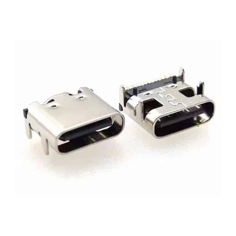
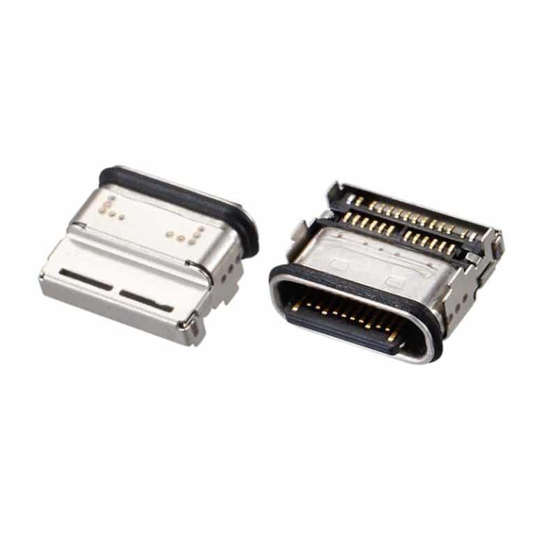
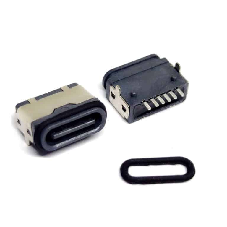
Signal integrity is the absolute core concern when designing PCB layouts for USB C PCB Connector (such as USB4 40Gbps). The requirements far exceed those for USB 2.0 or lower-speed USB 3.2, imposing extremely stringent specifications on impedance matching, crosstalk control, and loss.
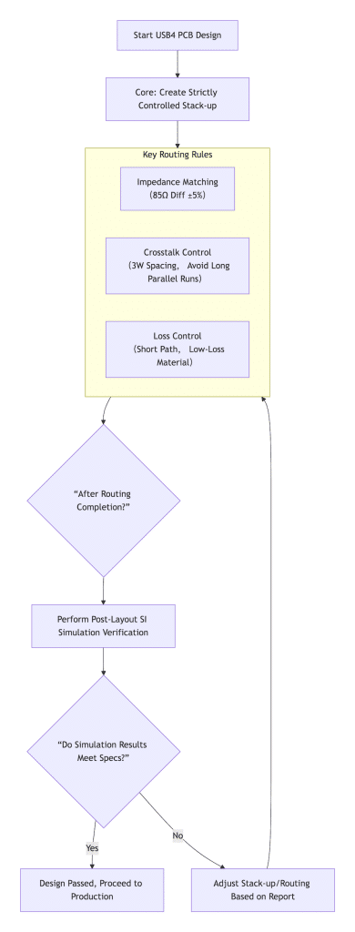
The following design guide details these specific requirements, accompanied by a design decision flowchart to aid your understanding.
Core Requirements and Specific Design Parameters
USB4, based on the Thunderbolt™ 3 protocol, requires dual-channel, full-duplex differential signal transmission. This means there are 4 pairs of ultra-high-speed differential lines, and each pair must perform nearly perfectly.
| Design Dimension | Core Objective | USB4 (40Gbps) Specific Requirements & Implementation Methods |
|---|---|---|
| 1. Impedance Matching | Ensure no signal reflection, maximize energy transfer. | Differential Impedance: 85Ω ±5% (Standard value, not the traditional 90Ω). • Implementation: Work closely with your PCB fabricator. Use their stack-up calculation tools to precisely calculate and specify trace width and spacing based on your chosen laminate (e.g., Megtron 6), dielectric constant (Dk), and layer thickness. |
| 2. Crosstalk Control | Prevent adjacent signal lines from interfering with each other. | Adhere to at least the “3W” Rule: Edge-to-edge spacing between adjacent differential pairs ≥ 3x the differential trace width. • Implementation: Place solid GND guard traces between RX/TX pairs; Avoid long parallel runs of high-speed lines with other clocks/periodic signals; Use stitching via arrays to surround signals in a Faraday cage. |
| 3. Insertion Loss | Control signal attenuation during transmission. | The total channel loss (connector + cable + PCB) has a strict budget. The PCB portion must be minimized. • Implementation: Use ultra-low-loss laminate materials (e.g., Panasonic M6, Rogers RO4350B); Minimize trace length (absolute max length depends on material, often needs to be <15cm); Avoid using vias. If vias are unavoidable, back-drill (stub removal) technology must be used. |
| 4. Intra-Pair Skew | Ensure differential signals arrive simultaneously to cancel common-mode noise. | Intra-pair length matching tolerance ≤ 0.15mm. • Implementation: Use tuning serpentines during routing for precise compensation, ensuring absolute length equality between the P and N lines of a pair. Compensation should be placed in straight, symmetrical sections of the trace. |
| 5. Inter-Pair Skew | Ensure data synchronization across multiple pairs in the same channel. | Length deviation between TX pairs and between RX pairs within the same lane must be tightly controlled (typically ≤ 1.0mm). • Implementation: Define inter-pair matching networks clearly in the schematic and PCB, and set strict length matching rules. |
PCB Layout and Routing Practical Guidelines
- Stack-up Design is Foundational
- You must plan an impedance-controlled stack-up with your manufacturer upfront. A minimum of 6 layers is recommended to provide complete reference planes for high-speed signals.
- Typical structure:
Top Layer (Signal) / GND / Power / GND / Signal / Bottom Layer. Ensure high-speed traces are routed on the top or bottom layer, adjacent to a solid, unbroken GND plane as a reference.
- Connector Region and Fanout
- The high-speed pins of the USB C pcb connector are very dense. The fanout area is the most challenging part.
- Impedance control must begin immediately as traces exit the connector pins. Traces should transition to inner layers as soon as possible, and surface layer routing should be kept as short as possible to reduce radiation and loss.
- Allocate sufficient space for each differential pair to avoid crosstalk starting in the fanout region itself.
- Judicious Use of Vias
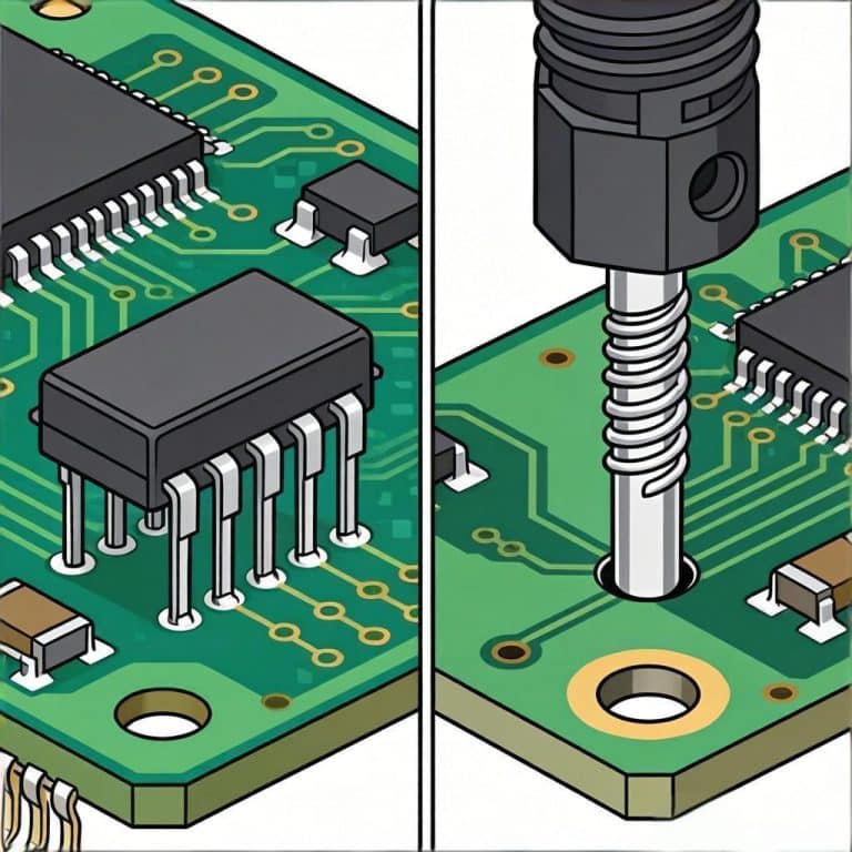
- Avoid using vias whenever possible. If a layer change is necessary (e.g., from the connector’s top side to bottom), use micro-vias or back-drilled vias.
- Each via introduces an impedance discontinuity and signal reflection, which is significant at 40Gbps speeds.
- Power Integrity and Decoupling
- The power supply for high-speed transceivers must be extremely clean. Place decoupling capacitors of multiple values (e.g., 10uF, 1uF, 0.1uF, 0.01uF) very close to each power pin of the chip to filter broadband noise.
- Provide a low-impedance power return path for the high-speed circuitry.
Verification: Simulation and Testing
Designing without simulation is designing blind.
- Pre-layout Simulation: Before routing, use SI tools to simulate the topology (driver, transmission line, receiver) of critical networks to predict performance.
- Post-layout Simulation: After completing the layout, extract the actual routing parameters (S-parameter models) and run simulations to check if eye diagram metrics like eye height, eye width, and jitter meet the USB4 specification.
- Physical Testing: Once prototype boards are produced, high-speed oscilloscopes and vector network analyzers must be used for compliance testing.
In summary, designing a USB4 PCB is a contest against physical limits. The keys to success are: starting with the correct stack-up and materials, adhering to extreme routing rules, and concluding with rigorous simulation and verification. Compromising on any of these aspects can lead to link failure.
If you can provide a more specific application scenario (e.g., motherboard, dock) or particular challenges you are facing, I can offer more targeted analysis. And if you want to know more about the USB C PCB connector, this video about complete analysis of USB Type-C interface signals and key points for PCB design may be helpful.

