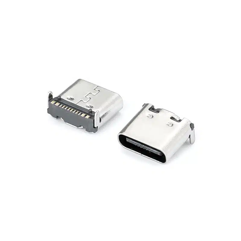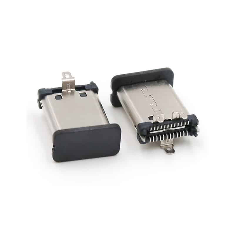
Understanding the differences in PCB layout between the USB-C 24-pin full-featured and 16-pin USB 2.0 connectors is crucial for ensuring stable device performance. The main distinction lies in the support for high-speed signal lanes, which directly impacts the complexity of layout and routing. The following table compares their key design points.


| Design Consideration | USB-C 24-Pin (Full-Featured) | USB-C 16-Pin (USB 2.0 Type) |
|---|---|---|
| Core Functionality | Supports USB 3.2/4 (5/10/20 Gbps+), DisplayPort Alt Mode, high-power PD (up to 240W), etc. | Supports only USB 2.0 data (up to 480 Mbps) and power delivery. |
| Differential Pairs | 8 pairs total. 4x SuperSpeed RX/TX pairs (SSTX/SSRX) + 1x USB 2.0 pair (D+/D-) + Auxiliary pairs (SBU). | 1 pair total. Only the USB 2.0 pair (D+/D-). |
| High-Speed Diff Pair Routing | Critical & Complex. 90Ω impedance (±10%). Length matching within pair (≤5 mils) and between pairs for RX/TX groups (e.g., ≤50 mils). Must be routed as diff pairs from connector to termination/IC with minimal vias (≤2). Requires continuous reference GND plane, no splits under traces. | Not applicable. |
| USB 2.0 Diff Pair Routing | Required, but lower priority. Route after high-speed pairs. 90Ω impedance. Length matching within pair (≤10 mils). | Core & Critical. Follow same rules: 90Ω impedance, length matching. |
| CC Pin Design | CC1 and CC2 are vital for mode detection and PD communication. Must have clean, direct routing to CC logic/PD controller. Use series resistors (typically 5.1kΩ pull-downs) placed close to the connector. Consider protection (TVS). | Same importance. Essential for establishing basic power contract and orientation detection. Same routing and pull-down resistor requirements apply. |
| Power Pins (VBUS) | Must support high current (e.g., 5A). Use wide traces/polygons based on current density (IPC-2152). Multiple VBUS pins may be paralleled. Place bulk and ceramic capacitors (e.g., 100µF + 0.1µF) close to connector. | Typically lower current, but still design for intended load (e.g., 3A). Follow same practice of adequate trace width and local decoupling. |
| Protection Circuit Layout | High-speed lanes: Ultra-low capacitance (<0.5pF) TVS diodes or ESD arrays, placed immediately at connector pads. For EMI, common mode chokes (CMC) placed after TVS but before series AC caps. VBUS: High-power TVS or surge protectors. | USB 2.0 lines: Standard/low-cap ESD protection. VBUS protection similar, depending on power level. Sequence: Connector → TVS/ESD (closest) → possible CMC/Filter → series resistors (if any) → to IC. |
| Auxiliary Signals (SBU) | Required for Alt Modes (e.g., DP, Audio). Route as controlled impedance single-ended lines. Often need ESD protection. | Not present. No routing needed. |
| Shielding & Grounding | Metal shell must be firmly connected to chassis/board ground (PGND) via multiple low-inductance paths (stitching vias, grounding clips). Maintain a gap (1-2mm) between PGND and digital signal ground (DGND), connected at a single “star” point near power entry. | Same requirement for shell grounding to ensure EMI shielding and mechanical stability. |
Expanded Discussion on Key Design Points
1. The Core Challenge: Signal Integrity for High-Speed Lanes (24-pin only)
This is the most critical and differentiating aspect. Each of the four SuperSpeed differential pairs (SSTX1/2, SSRX1/2) carries multi-gigabit signals.
- Impedance & Stackup: The 90Ω differential impedance must be calculated with your PCB fabricator, considering trace width/ spacing, dielectric thickness (H1), and material (e.g., FR4). A controlled impedance stackup is mandatory.
- Length Matching: Mismatches cause intra-pair skew, degrading the signal eye diagram. Intra-pair matching (difference between P and N) must be extremely tight (<5 mils). Inter-pair matching (e.g., all TX pairs to each other) is also needed for bus alignment, with tolerances defined by your host controller (typically 50-150 mils).
- Reference Plane & Crosstalk: The pairs must have an unbroken, continuous ground plane directly underneath (on the adjacent layer). Avoid routing other signals, especially clocks, parallel to these pairs for long distances. Maintain at least 3x the trace width spacing from other aggressive signals.
2. Power Integrity: Handling High Current (Applicable to Both, Critical for 24-pin)
USB PD can deliver up to 48V/5A (240W). Even for lower power, proper design is key.
- Trace Width Calculation: Don’t guess. Use an IPC-2152 calculator. For 5A on a 1oz external layer, a trace width of over 100 mils may be needed. Often, using a power polygon on a dedicated layer is the best solution.
- Local Decoupling: The purpose of the capacitors near the VBUS pins is to handle instantaneous current surges when a device is plugged in and negotiates power. A bulk electrolytic (e.g., 47-100µF) handles low-frequency surges, while a ceramic (e.g., 10µF 0805/X5R) handles high-frequency noise.
3. ESD and EMI Protection Strategy
- Protection Placement: The golden rule for ESD protection is “as close to the point of entry as possible.” The TVS diode should be within 1-2mm of the connector pad. Long traces before the protection device act as antennas, rendering it ineffective.
- Component Selection for 24-pin: For SuperSpeed lines, the parasitic capacitance of the TVS diode is paramount. Capacitance >1pF can severely attenuate high-frequency signals. Select specialized, low-cap ESD diodes (e.g., <0.5pF).
- Chassis Grounding: The connector shield’s connection to the chassis ground is a primary path for ESD and EMI energy to be safely shunted to earth, protecting the internal ICs.
Design Flow and Selection Guide of USB-C 24-Pin Full-Featured and 16-pin USB 2.0

How to Choose:
- Choose 24-pin Full-Featured: If your device requires fast data transfer (external SSDs, high-res cameras), video output (docks, monitors), or the latest high-power USB PD.
- Choose 16-pin USB 2.0: For devices like keyboards, mice, low-speed sensors, chargers for non-critical devices, or any application where cost, board space, and design simplicity are primary drivers, and high-speed data/video is unnecessary.
Recommended PCB Layout Design Flow (for 24-pin):
- Placement: Position the USB-C connector at the board edge. Place the associated PD controller, high-speed multiplexer (for Alt Mode), and ESD protection diodes as close as possible to the connector.
- Routing Priority (Highest to Lowest):
- SuperSpeed Differential Pairs: Route these first, with strict impedance and length controls.
- USB 2.0 Differential Pair: Route next.
- CC, SBU Lines: Route as direct, clean traces.
- VBUS Power Planes: Create wide polygons or thick traces.
- Grounding: Ensure solid ground plane and shield connection.
- Post-layout Verification: Use your PCB tool’s Signal Integrity (SI) and Design Rule Check (DRC) features to verify impedance, length matching, and clearances. A 3D model check can also help avoid mechanical conflicts with the connector housing.
This detailed comparison and expanded guidelines should provide a solid foundation for your PCB design. If you encounter more specific challenges in your application, such as dealing with specific layer stack-ups or EMI filter selection, further detailed discussion is possible. More info, you can refer to What is the difference between 16-pin and 24-pin for USB type-C?.